This project is about interfacing:
A Simple Line Follower
The first simple roboter is running - a line follower. An exercise that kids solve in an hour. I needed a little bit longer because I had to solder some components, drill holes, write VHDL code and a few lines of Java ;-)
A small movie: linefollow.mov
Interfacing the Sensors
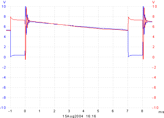
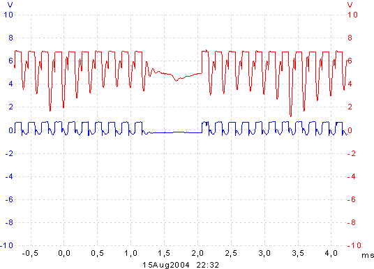
Figure 1 shows how the RCX interfaces with the LEGO sensor.
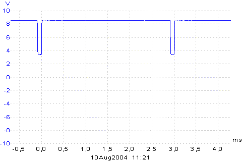
We can see the 3ms periode where the sensor is powered for about 2.8ms.
The power is switched off for about 200us and a 0-0.4mA current sink
provides the output signal. The voltage is generated by a pull up resistor
to 5V.
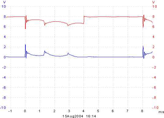
Figure 2 showes the schmatic for the FPGA sensor interface.
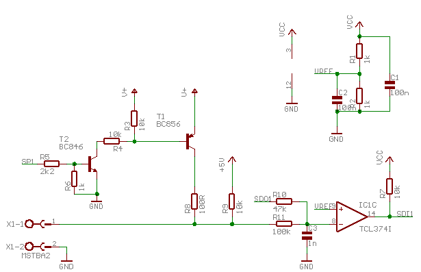
T1 and T2 are switched by the FPGA output SP1 to power the sensor with the
unregulated voltage (V+). When switched off, the current sink will generate
a voltage on the 10k pull up (R9 to the regulated 5V). R10, R11, C3 and IC1
build the integrator and comparator for the sigma-delta ADC in the FPGA.
SDO1 is driven by the FPGA and SDI1 is the input. VCC is 3.3V, the IO-voltage
typically for most FPGAs.
lesens.vhd is the VHDL module for the interface.
The sensor is powered for about 1.5ms. During the next 0.25ms the voltage
over C3 will settle to the correct Vref level. The value of SDI is integerated
(a nice word for counting 1s) in the FPGA during the next 0.25ms.
We get a new sensor value every 2ms (exact 2048 us).
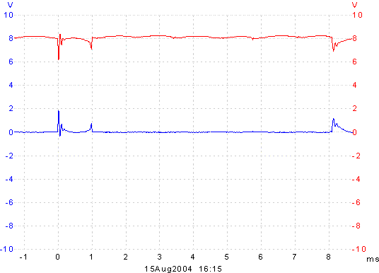
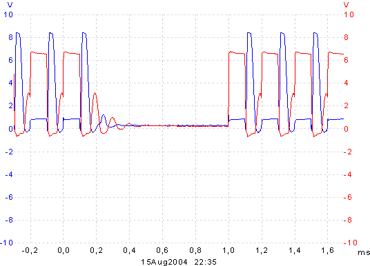
Figure 3 shows the osci plot of the FPGA interface.
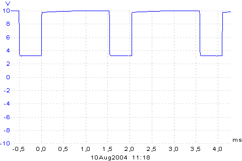
The 9-bits ADC could generate values from 0 to
511. However, the values of R9, R10 and R11 limit the range: 130 (on a short
curcuit) to 447 (leaving the input open).
Following Java fragment shows the test loop with a conversion of the 0-5V
input voltage to a 0-100 range:
        for (;;) {
            // 0V ... 130 (short)
            // 5V ... 447 (open)
            int v = Native.rd(Const.IO_ADC1)-130;

            v *= 81;    // v = v/3.17
            v >>>= 8;
            if (v<0) v=0;
            if (v>100) v=100;
            Dbg.intVal(v);

            RtThread.sleepMs(500);
        }
Motor Driver
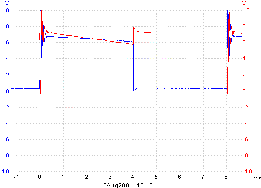
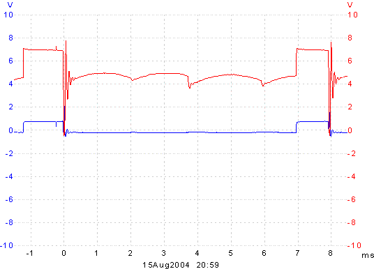
First we will take a look how the RCX drives the motor. Figure 3 shows a free running motor with power level 1. The startup can be seen in Figure 4 and a blocked motor is shown in Figure 5. All oscilloscope figures show both motor outputs with respect to battery ground.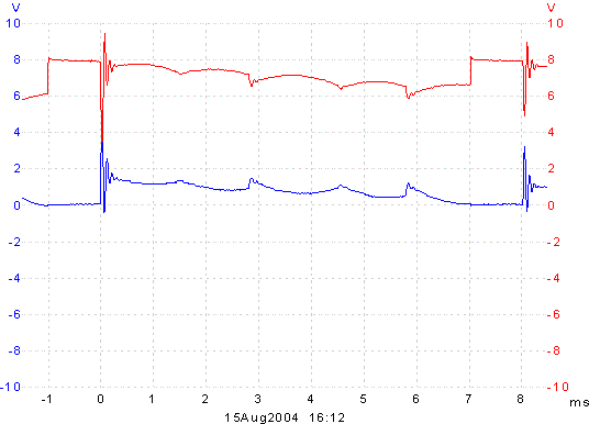
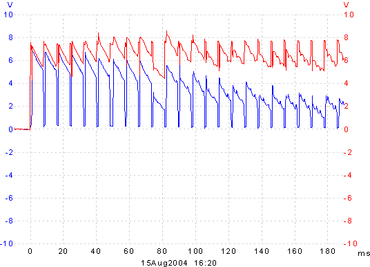
The RCX uses simple PWM with a period of 8ms (= 125Hz) and 8 steps of 1ms.
As we can see from the voltage levels during the off part of the PWM both
output drivers are disabled. However, when the RCX shuts the motor off both
drivers are active low to break the motore.
In the off phase we can see the back-EMF as the difference between the two
voltage lines. We see the acceleration during motor start and the zero
velocity when the motor is blocked.
Figure 6 to Figure 11 show the same measurements with power level 4 and 7.
At power level 8 the drivers are continuously enabled; not an interesting
measurement.
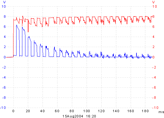
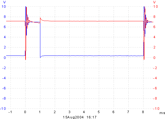
When comparing Figures 4, 7 and 10 we see the difference in the acceleration.
The final velocity is allmost the same for all power levels for a free
running motor.
The voltage drop on the output transtors can be seen with the blocked motor:
Less than 1V on the high-side transistor and about
0.5V on the low-side transistor.
A very simple schematics for the output stage is shown in Figure 12.
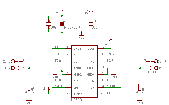
The L293 is an old and therefore common part.
The input levels of the L293D are 3.3V compatible and it has integrated
clamp diodes, thus making the interface from the FPGA to the motor trivial.
The main disadvantage of this part are the bipolar push-pull outputs having
a large voltage drop compared to a FET output stage.
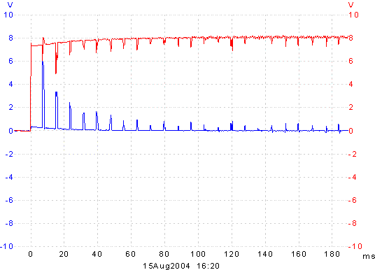
To make the motor driver more interesting we add two ADCs (Figure 13) to
measure the back-EMF when both drivers are disabled.
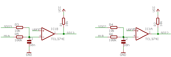
The ADC is our workhorse sigma-delta ADC. The main difference to the former
ADC is the the higher ratio of the two resistors. With the ratio of 10 the
input range is between -14.85V and 18.15V (-1.65V*10 + 1.65V and 1.65V*10 + 1.65V).
The pull-down resistors R1 and R2 in Figure 12 avoid floating levels when both outputs
are tri-stated.
We will check our driver with the same PWM as the RCX generates. Figure 14 and
15 show the free running and stalled motor with a PWM of ratio 1:8.
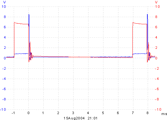
There is no VHDL file for this PWM as it was simpler to generate it in Java
and JOPs scheduling is fast enough for this timing ;-)
The drivers where powered with the RCX battery pack to provide comparable
measurements.
The figures are very similar to the one taken with the RCX. The main difference is the
higher saturation voltage of the output transistors and that one output is
tied to ground during the off phase.
The PWM frequency of the RCX is quite low. We will change this, but add a longer off-time from time to time for the back-EMF measurement. Figure 16 shows one example.
This example is still done in Java. A VHDL version generating this PWM and triggering the sigma-delta ADC will follow.
-- stay tuned --
Now it's time to play some LEGO! I should build my first simple robot and let JOP control it before I move on with the back-EMF stuff ;-)
References
There are a lot of good websites available about the internals of the LEGO MindStorms, substitutes for the RCX operating system (even a small JVM is available) and how to build your own sensors.Here are only a few links, that where helpfull to build the FPGA interface.
Larry Barello has a good introduction how LEGO sensors work.
A lot of information can be found at Michael Gasperis sensor page.
Acroname has a good explanation how back-EMF measurement.
Systronix builds a substitute for the RCX, called JCX. It consists of peripheral prints for the aJile Java processor powered JStamp. In my opinion they are using too many hardware components. However, they are providing the schematics of their board, a nice gesture.
Conclusion
As I'm currently building the system it's too early to draw conclusion ;-)Contact
If you have comments or suggestions please drop me a note: martin@jopdesign.comIf there is enough interest in a PCB that contains the FPGA interface I will probably route one.